CeNTech R & D
Dr. Harry Mönig
Center for Nanotechnology (CeNTech),
University of Münster
Heisenbergstr. 11, D - 48149 Münster
Phone: +49 (0)251/ 83-63832
Fax: +49 (0)251/ 83-63873

Research Focus: Nanoscale Interface Analytics
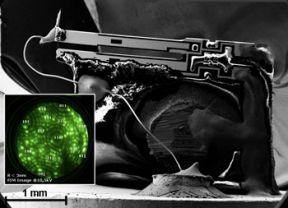
 Scanning electron microscopy image of a tuning fork sensor for simultaneous nc-AFM/STM experiments. Inset: tip-apex characterization by field ion microscopy.
To take account for an increasing need for a knowledge based material and device design, there is a high demand for analytical investigations on an atomic scale. The work in our group aims to understand processes at organic, inorganic and hybrid interfaces that are relevant for the performance of optoelectronic devices such as solar cells or light emitting diodes. Within our projects, we apply scanning probe microscopy methods with a focus on non-contact atomic force microscopy (nc-AFM), where we perform local force spectroscopy, energy dissipation, and contact potential difference measurements. Furthermore, our instrumentation allows to record tunneling currents, which enables us to perform simultaneous nc-AFM and scanning tunneling microscopy (STM) measurements. We utilize the different topographic and spectroscopic information channels to gain access to the interface properties with a spatial resolution down to the picometer range. The investigations are performed under ultrahigh vacuum (UHV) conditions and at low temperatures to establish highly defined experimental conditions.
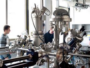
 Combined ultrahigh vacuum system with a tuning fork based low temperature atomic force microscope (left part) and an interconnected photoelectron spectroscopy set-up with UV- and monochromatic X-ray sources (right).
Complementary to our scanning probe microscopy experiments we perform photoelectron spectroscopy (PES) to investigate interface properties with respect to chemical binding, composition, and band alignment. Our PES set-up is directly coupled to the nc-AFM system allowing the transfer of samples from the one to the other experiment without breaking the vacuum. The PES set-up is equipped with a three dimensional delayline detector, which allows to record images of the angular distribution of photoelectrons. This provides access to the band dispersion of electronic states (e.g. of functional organic layers, inorganic thin films, or adsorbate-induced states). PES can also provide depth dependent compositional and chemical information of the samples under investigation.


